© Universität Bielefeld / André Wirsig

Equipment
Thin film deposition
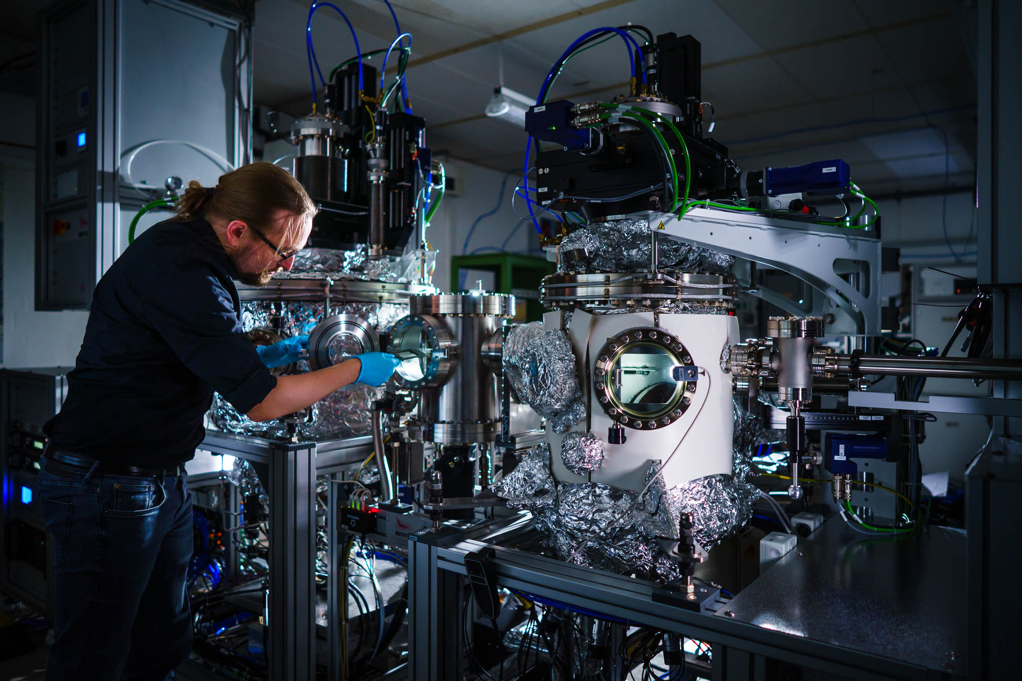
BESTEC thin film deposition system
- ultra high vacuum system with loadlock
- vacuum chamber for magnetron (co)-sputter deposition (DC or RF mode)
- vacuum chamber for molecular beam epitaxy
- sample heating (up to 1000°C)
- in-situ resistance and magneto-resistance measurements
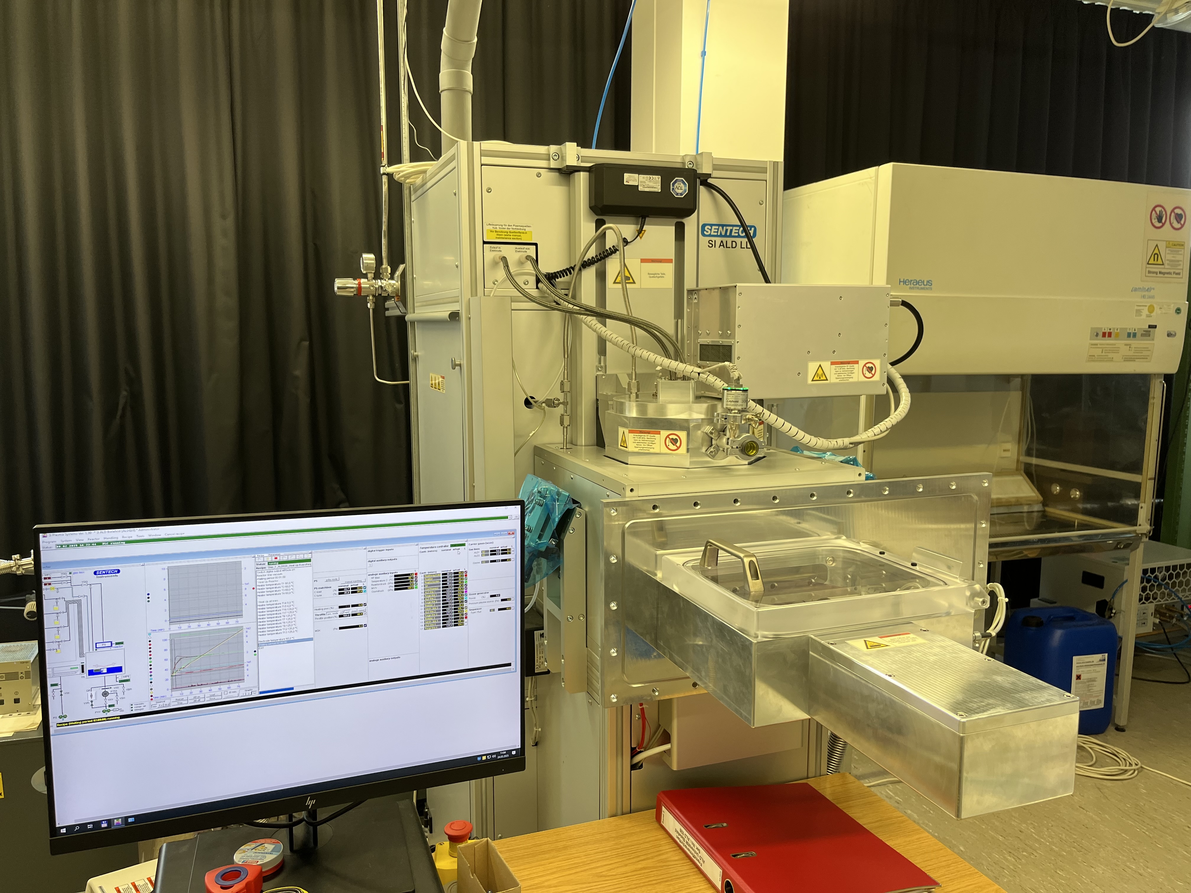
SENTECH atomic layer deposition system
- thermal and plasma enhanced deposition
- up to 100mm samples
- deposition temperatures from room temperature up to 300℃
- extremely uniform and conform oxide- and nitride-layers
BesTec 3 inch Co-Sputtering System
- sputter deposition
- eight three inch sources, DC or RF mode
- ultra high vacuum
- sample heating (1000°C) and rotation
- 10 kW electron beam evaporator
- 1kW rapid thermal annealing unit
Leybold CLAB600
- sputter deposition
- six four inch sources, DC or RF mode
- high vacuum
- automatic sample handling
- plasma oxidation chamber
Microscopy and Lithography
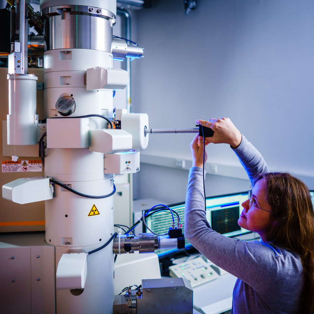
Transmission electron microscopy
FEI Helios NanoLab DualBeam Focused Ion Beam
- Ga ion beam
- nano-manipulator
- scanning electron microscope
- EDX for mapping
- 3D tomography
Zeiss LEO 1530 Scanning Electron Microscope
- 5-20kV operating voltage
- high vacuum
- EDX detector
- Raith laser interferometer sample stage for electron beam lithography
Scanning Auger microscopy
- Physical Electronics Phi660
- surface sensitive analysis of composition
- depth profiling (Ar ion etching / spectroscopy), Zalar rotation for optimized depth resolution
Ion Beam Etching system
- low-voltage ion beam (up to 1.2keV)
- ultra high vacuum
- secondary ion mass spectroscopy (SIMS) for in-situ monitoring of the etching depth
Analytics
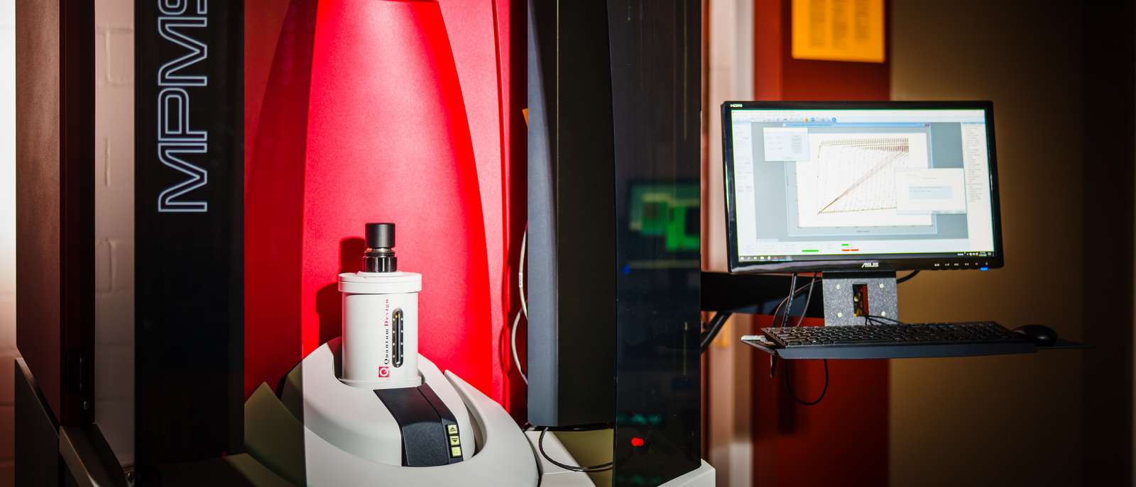
3rd Generation MPMS SQUID Magnetometer (Quantum Design)
- with evercool close-cycle system - 7.0 Tesla magnet
- vibrating sample magnetometer (VSM) extraktions Modus
- electrical transport option (ETO) for MPMS3

Philips X'Pert Pro MPD x-ray diffractometer
-
theta-2theta geometry
-
Cu K-alpha source
-
Bragg-Brentano optics
-
open Euler cradle
-
LN2 chamber for cryo measurements
-
x-ray reflectivity (XRR)
-
small angle x-ray scattering (SAXS)
-
https://en.wikipedia.org/wiki/X-ray_reflectivity
x-ray fluorescence (XRF) analysis of composition of thin films and bulk samples
- Amptek XR-100CR x-ray fluorescence detector
- Amptek Miniature x-ray source (Ag), 10keV to 50keV
- He atmosphere in the sample space for elements down to Al
Magneto-optical Kerr effect (MOKE)
-
Vector MOKE:
-
3-axis magnet (0.35T)
-
perpendicular or 45° incident light
-
sample rotation and heating
-
Kerr rotation and ellipticity
-
different wavelengths
-
-
2T MOKE:
-
Bruker electromagnet (up to 2T)
-
polar and longitudinal geometry
-
650nm Laser
-
s- or p-polarized incident light
-
Cryogenic Ltd. Cryostat system
- closed cycle He cryostat (1.2 K)
- 3He dilution insert (0.3K)
- 4T superconducting magnet + 0.5T transverse field
- for all kinds of temperature dependent transport measurements
Atomic Force Microscope Bruker Multimode 5
- tapping mode & contact mode
- magnetic force mode (MFM)
- conducting AFM
Variety of setups for...
- temperature dependent magneto-resistance measurements
- spin-transfer-torque measurements
- spin-orbit-torque measurements
- spin-caloric characterization (rotatable thermal gradients up to 30K in rotatable magnetic fields of up to 0.1T)
- ...
Introduction to the field:
Phone- and room numbers of our main laboratories
Labs at D2 (main university building):
Sputter deposition and ALD: 2585, D2-262
Thin film deposition (CLAB600, MBE): 2617, D2-229
X-ray reflectivity, diffraction, fluorencence: 5409, D2-244
Labs at D02 (main university building):
AES and calorimetry: 2511, D02-225c
AGM and thermal gradients setup: 12729, D02-202
Labs at E0 (XPhy bulding):
REM: 12563, XPhy E0-308
FIB: 12566, XPhy E0-405
Technical room REM/FIB: 12683, XPhy E0-307
TEM: 12564, XPhy E0-311
Technical room TEM: 12685, XPhy E0-312
Clean room: 12567, XPhy E0-406
Sluice of the clean room: 12684, XPhy E0-310
Labs at E1 (XPhy bulding):
Magnetic setups I: 12589, XPhy E1-405
Magnetic setups II: 12592, XPhy E1-408
Cryo lab / Deposition: 12590, XPhy E1-406
Central preparation: 12591, XPhy E1-407
AFM / STM: 12593, XPhy E1-409
Thermoelectric lab: XPhy E1-309
Technical room Thermoelectric lab: XPhy E1-310
Tea kitchen: 12569, XPhy E1-106
General phone numbers (XPhy bulding):
Foyer info point: 12649
Foyer door: 12650
Communication zone 1st floor: 12651